Do you want to buy antibiotics online without prescription? https://buyantibiotics24h.net/ - This is pharmacy online for you!
An-5013 gtlp in btl applications
GTLP in BTL Applications Abstract Compatibility BTL Appli
Today’s high performance systems require fast edge rates
Because GTLP is an evolutionary step from the previous
and smooth transitions with minimal ringing, overshoot/
designs in BTL and ECL, it shares many of the conceptual
undershoot, and other signal integrity issues. The Gunning
features and performance characteristics that multi-drop
Transceiver Logic Plus (GTLP) family offers a portfolio of
applications require. Since the GTLP family provides bi-
translation devices and clock drivers that are not only capa-
directional translation of LVTTL signal levels and GTLP sig-
ble of the fast HL/LH transitions demanded for high speed
nal levels, there are varied requirements when driving or
backplanes, but also feature a unique edge rate control
receiving signals from either of its interface ports. Some of
characteristic that ensures smoother transitions. By tuning
the desirable features of the GTLP port driver include high
the backplane with proper termination resistors and refer-
drive capability, low output impedance, controlled output
ence voltage techniques, GTLP can act as a drop-in electri-
edge rates and live insertion characteristics. It must also
cal solution for Backplane Transceiver Logic (BTL) as well
provide a completely different set of characteristics for the
as support high-speed backplane systems up to 125 MHz
LVTTL driver interface such as medium drive levels,
and beyond. GTLP’s real advantages occur when the
devices are operated at their recommended normal operat-ing specifications. This application note illustrates the abil-
Specifications
ity of GTLP to perform in existing BTL applications andevaluates GTLP port interface equivalence with most fami-
One of the noted differences between BTL and GTLP is the
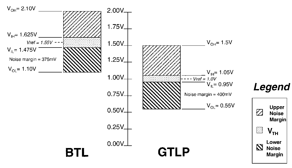
output and input signal. As depicted in Figure 1, BTL andGTLP differ in their drive and threshold levels. This may
Background
seem like a major design problem, when in fact GTLP canoperate at the I/O levels specified by BTL. At these levels,
BTL and GTLP signaling can be seen as derivations of
the drive characteristics of two technologies look very com-
ECL/PECL signaling. Each of them addresses “open col-
patible. The output IOL characteristics of BTL and GTLP
lector” or “open drain” control of a multi-drop signaling envi-
can be plotted together. The curves in Figure 2 show that
ronment with the benefit of a pull-up termination for output
GTLP has stronger drive at the critical low output voltage
high signal levels. The benefit of “open drain” technology is
levels. The stronger drive will provide more noise margin
that the output is either sinking current or in high imped-
ance state (3-STATE) but never sources current. It can alsoprovide translation from TTL/LVTTL signaling.
The evolution from ECL to BTL to GTLP was an effort tosolve power consumption problems in earlier applicationswhile providing near-equivalent performance. ECL is apure bipolar design and BTL designs are BiCMOS. GTLPwas the first all CMOS solution and provides the mostpower savings of the two previous device designs. FIGURE 1. Input/Output Signal Level Comparison
2001 Fairchild Semiconductor Corporation
Specifications (Continued) Throughput/Performance
Using GTLP at BTL voltage levels results in a maximumfrequency similar to BTL of about 40 MHz. When used atthe recommended voltage levels, however, GTLP’s outputcontrol circuitry allows operation at frequencies exceeding100 MHz.
By controlling the device’s output edge rate, much lessovershoot and undershoot characteristics are seen thanwith fast signal transitions in medium to high performancebackplanes. The ability to set different rise and fall timescompensates for various loads. Therefore the output edgerate control feature coupled with an adequate terminationscheme allows the system designer to fine tune the outputedge for optimum performance. Such features are foundon the GTLP16T1655. FIGURE 2. Output I
Proper termination of the system is important for optimizing
OL Characteristics
performance. The backplane impedance will vary from sys-
From a datasheet point of view, GTLP and BTL provide dif-
tem to system depending on stub lengths, number of slots,
ferent reference from which they derive their specifications.
slot pitch, and types of connectors used. The recom-
BTL follows the standards set by various standards’ bodies
mended termination technique for GTLP is a Thevenin ter-
and its specifications are set by those. GTLP is more flexi-
mination. This termination scheme uses two resistors in
ble in which standard it needs to set its specification. Ini-
parallel, one at each end of the backplane. The resulting
tially GTLP followed an established specification set by
parallel value of the resistor equals half that of the trans-
Intel in their microprocessor interface designs. Intel set
mission line. This type of termination reduces overshoot
these specifications in an effort to optimize on-board signal
and improves the noise margin of the system, both of
integrity characteristics. However, off-board applications
which are critical for incident wave operation.
remain more “open” in nature, and the flexibility of theGTLP output allows it to interface to a number of interfacesignal levels. Power Consumption
Interface signals in today’s high-speed systems often have
The output structure of GTLP is designed for a 50Ω termi-
to contend with edge rates becoming faster and refections,
nation tied at each end of the backplane. This parallel ter-
ringing, crosstalk, and ground bounce becoming more evi-
mination configuration is a 25Ω equivalent load. Single
dent. Interface signal levels, through their noise margins,
ended termination in a bi-directional backplane will result in
become important in ensuring system stability. GTLP
non-incident wave switching which can cause signal integ-
devices, such as the GTLP6C816, offer comparable noise
rity problems. With a 25Ω Thevenin equivalent load, the
margins to its BTL predecessors. The combination of a
static current demand with GTLP is 34 mA. Since BTL typi-
50mV threshold margin coupled with a wider V
cally has load impedances of 19.5Ω (39Ω/2 for parallel ter-
margin means GTLP can operate within BTL signal level
mination), the IOL is 51mA. Table 1 shows the relationship
specifications. Figure 1 shows the lower noise margin to be
between VOL and IOL with each technology.
400mV for GTLP compared to 375mV for BTL. TABLE 1. IOL Demand Voltage Levels Technology
BTL and GTLP both need a termination voltage (V
voltage pin (VREF) which is an input threshold voltage used
to reference an incoming BTL/GTLP signal. As a starting
Note 1: IOL = (VTT − VOL)/RT
point for prototype designs, Fairchild recommends that
Many factors, both internal and external, affect the power
VREF be generated from VTT with the use of a simple volt-
consumption of a device: (1) number of outputs simulta-
age-divider circuit. By tying VREF to VTT, at any point that a
neously switching, (2) operating frequency of the system,
signal falls below the threshold region, incident wave
(3) junction temperature, and (4) capacitive load. The out-
switching can still be achieved by lowering the VTT which
put power of both GTLP and BTL are supplied by an exter-
consequently lowers VREF. By centering the noise level
nal output voltage supply (VTT). When calculating the static
between VREF and VTT, the maximum noise immunity can
high power consumption of the device, the device power is
minimal during a static high event. This is because the out-
put is in the high impedance state, and essentially zero cur-
uses an external VREF pin, and it is recommended that it be
When considering static low drive current, the output power
is at the worst case point. As seen in Table 2, GTLP usesless power than its predecessor BTL does. The powerrequirement is increased when considering that two 8-bitBTL devices are needed for one 16-bit GTLP device. Power Consumpt Consumpt ion Continued) TABLE 2. Static and Dynamic Power Consumption Replacing BTL with GTLP
GTLP can be used in either high-speed new designs,where signal integrity and smooth edge transitions are cru-
cial, or as an electrical drop-in solution for an existing BTL
slot. The BTL family has many advantages over older
CMOS and TTL logic families when designing large back-
planes, and GTLP can be used in much higher perfor-
mance backplanes than BTL while offering many of the
BTL Appli Note 2: P = VCC*ICC + n* (VOL*IOL) where n = number of outputs
same characteristics. GTLP has the capability of operating
The dynamic power consumption comparison between
at a wide range of voltage levels without sacrificing signal
BTL and GTLP can be shown graphically as a load line cal-
integrity. GTLP can maintain adequate noise margin since
culation. The IOL curves in Figure 3 show this comparison.
VREF is derived from VTT. This flexibility allows GTLP to
The dynamic power consumption of the two technologies
are approximately the same given the same operating con-
Many BTL transceivers use a live insertion pin (LI) to sup-
ditions, and when GTLP is used at its recommended oper-
port hot swapping of cards without disabling the system.
ating conditions (1.0V for VREF) it uses much less power.
This is necessary in some applications when changing or
As previously discussed, GTLP offers twice the number of
adding daughter cards to a backplane. When the LI pin is
bits per device than the BTL technology does.
connected to VCC, the output Schottky diode is reversebiased which minimizes bus loading by reducing thecapacitance.
GTLP also supports live insertion applications. Forinstance, the GTLP16T1655 16-bit universal transceiverhas a VCCbias pin which forces 1V on the output pins. Bypre-biasing the output pins to 1V, the device will preventthe backplane from rail-to-rail voltage swings which causessystem problems upon live insertion of a daughter card. Conclusion Today’s high performance systems require fast edge rates and smooth transitions with minimal ringing, overshoot/ undershoot, and other signal integrity issues. The GTLP family offers a portfolio of translation devices and clock drivers that are not only capable of the fast HL/LH transi- FIGURE 3. IOL Characteristics with AC Load Line
tions demanded for high speed backplanes, but also fea-ture a unique edge rate control characteristic that ensuressmoother transitions.
By tuning the backplane with proper termination resistorsand reference voltage techniques, GTLP can act as a drop-in electrical solution for BTL as well as support high-speedbackplane systems up to 125 MHz and beyond. GTLP’sreal advantages occur when the devices are operated attheir recommended normal operating specifications.
Fairchild does not assume any responsibility for use of any circuitry described, no circuit patent licenses are implied andFairchild reserves the right at any time without notice to change said circuitry and specifications. LIFE SUPPORT POLICY
FAIRCHILD’S PRODUCTS ARE NOT AUTHORIZED FOR USE AS CRITICAL COMPONENTS IN LIFE SUPPORTDEVICES OR SYSTEMS WITHOUT THE EXPRESS WRITTEN APPROVAL OF THE PRESIDENT OF FAIRCHILDSEMICONDUCTOR CORPORATION. As used herein:
1. Life support devices or systems are devices or systems
2. A critical component in any component of a life support
which, (a) are intended for surgical implant into the
device or system whose failure to perform can be rea-
body, or (b) support or sustain life, and (c) whose failure
sonably expected to cause the failure of the life support
to perform when properly used in accordance with
device or system, or to affect its safety or effectiveness.
instructions for use provided in the labeling, can be rea-sonably expected to result in a significant injury to the
www.fairchildsemi.com
ANAT 2160/BIOL 3430 Nervous tissue and cartilage laboratory module 1) Nervous tissue Objectives: 1) understand the structure of neuronal somata (cell bodies) and cytoplasmic processes 2) identify somata and processes of neurons in other tissues in the body 3) identify cell types that support neurons in the central and peripheral nervous systems 4) understand the relationship between pe

 GTLP in BTL Applications
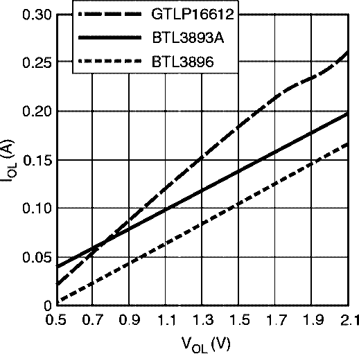 Specifications (Continued)
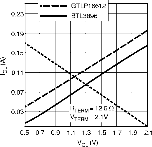 Power Consumpt